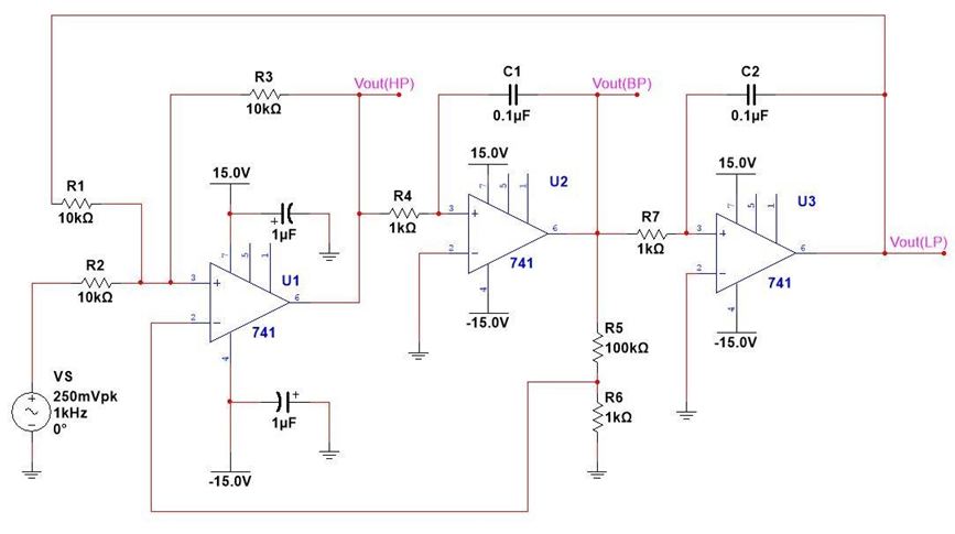
#1. State Variable Filter
This project implements a state variable filter (SVF) using three operational amplifiers to generate high-pass, band-pass, and low-pass outputs from a single analog circuit. Each op-amp stage performs a specific function, and together they form a flexible filtering system whose cutoff frequency and response are set by resistor and capacitor values. Because all three filter outputs are derived from the same internal signals, they remain mathematically related and consistent across the entire circuit.
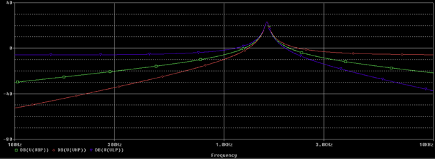
The SVF design allows multiple filter responses to be accessed simultaneously without requiring separate circuits for each type. By adjusting only a few component values, such as the internal resistors and capacitors, the filter’s cutoff frequency and quality factor can be easily tuned while maintaining stable and predictable performance. This makes the circuit well-suited for applications such as audio signal processing, synthesizers, and control systems, where flexibility and efficiency are important. The following graph shows the simulated results of the SVF circuit, where the blue signal shows the low-pass , green signal shows the band-pass, and the red signal shows the high-pass filtered results in the DB scale.
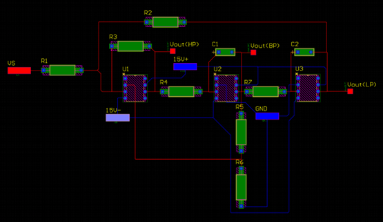
The circuit was implemented on a single-layer PCB using mostly through-hole components to simplify assembly, testing, and modifications. The board includes multiple test pads placed throughout the signal path, making it easier to probe signals and debug the filter stages during development. Inputs and outputs are provided as exposed copper pads for straightforward connections, allowing quick integration with external equipment such as signal generators, oscilloscopes, and simple audio test systems.
#2. Custom Microcontroller PCB Design
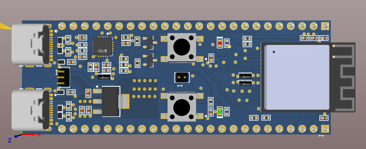
This project involved the complete design of a manufacture-ready, four-layer printed circuit board (PCB) centered around the ESP32 microcontroller, using Altium Designer as the primary CAD tool. The work began by completeing the schematic, where the circuitry is separated into functional blocks such as power regulation, USB communication, programming interface, and core microcontroller connections. Custom schematic symbols and PCB footprints were created and verified against manufacturer provided datasheets and common industry practices to ensure dimensional accuracy, readability and pin compatibility. Throughout the design process, each component's datasheet recommendations were followed, particularly for USB-C connection ports, USB to UART module, microcontroller's power and ground routing , as these directly affect reliability and performance in real hardware.
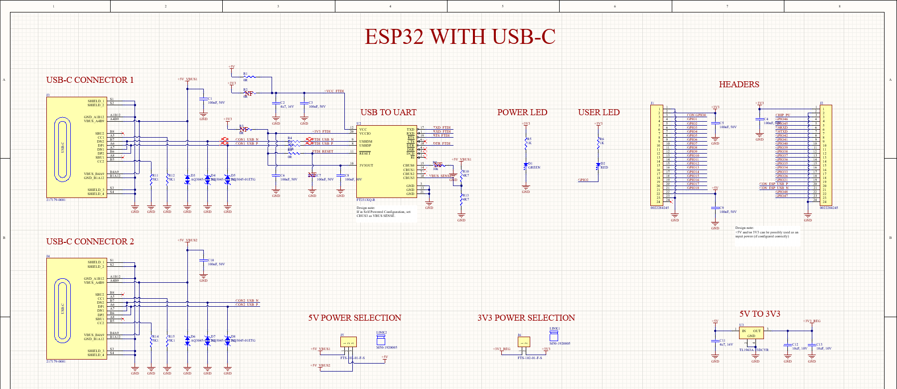
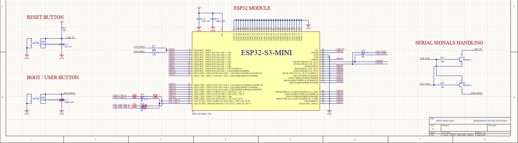
A critical design decision in this project was the use of a four-layer stack-up consisting of Top Signal, 3.3 V Power, Solid Ground Plane, and Bottom Signal layers. This controlled stack-up improves signal integrity, and routing efficiency by providing space for both wider traces for high amperage power paths and shorter paths routed away from power paths which reduces electromagnetic interference (EMI). The dedicated ground plane reduces noise coupling and ensures stable reference voltages, while the internal 3.3 V power layer improves current distribution and reduces voltage drop across the board. This structure is especially important for the ESP32 and USB interfaces, which operate at relatively high frequencies and are sensitive to poor grounding.
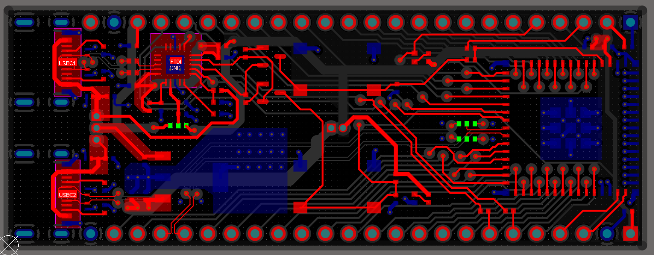
The figure shows the top layer of the PCB showcasing signal and 5V power connections in red and ground connections in blue.